How Does PCB HDI Support Advanced Semiconductor Packaging?
PCB HDI Support
PCB HDI supports advanced semiconductor packaging, allowing components to be packed closer together with greater functionality and speed. It also offers more efficient power distribution and thermal management, while remaining small and lightweight. This technology requires specialized expertise to design correctly and optimize the board for performance. Moreover, it demands precise manufacturing processes to create high-quality boards that are robust and reliable.
The fabrication process for HDI circuit boards involves several intricate steps, including microvia drilling and sequential lamination. This is a crucial step in creating the high-density interconnects that are essential for HDI boards to function properly. Microvia drilling is done using lasers, which drill extremely fine holes to establish connections between different layers of the board. The subsequent step of sequential lamination involves layering thin sheets of insulating material and copper foil to build up the board’s structure.
Microvias are a critical component of the pcb hdi and play an important role in determining the signal transmission quality of the circuit board. Using the right stack-up and construction, they can provide more pins per square inch than standard through-hole pins and reduce signal delays. Additionally, the thinner dielectrics that are used with the microvias can aid in heat dissipation.
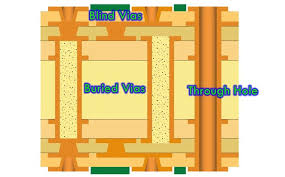
How Does PCB HDI Support Advanced Semiconductor Packaging?
When designing a circuit board, it’s important to consider the manufacturability of the components and the layer count of the board. It’s also vital to understand how the various via types and stack-ups can affect routing density. The type and amount of vias, through-holes or microvias that are needed will impact the cost of the board, so it’s important to select a fabricator that can offer cost-effective solutions.
Sierra Circuits provides an HDI stack-up tool that enables designers to play around with different via configurations and layouts to determine the minimum routing density required for their design. The tool allows users to define trace widths, via diameter and location, and pad size. It also helps them to decide the best configuration for their project’s requirements and determine the optimum layer count.
It’s vital to consider the materials used to fabricate the circuit board when deciding on an HDI design. Choosing the right material can have significant effects on signal integrity, temperature stability, mechanical strength and reliability. This is especially true when evaluating the core substrate material, which must have a low dielectric constant and be resistant to corrosion.
The type of copper plating also has a huge impact on the overall performance of a circuit board. There are two primary types of copper plating, electroless and electrolytic, which each have their own unique benefits. While the former is more cost-effective and environmentally friendly, the latter offers superior conductivity and durability.
The selection of the right PCB supplier is also key to ensuring cost-effectiveness. A quality manufacturer that offers quick turnaround and fast customer service can help reduce costs. Additionally, working with a supplier that uses a proprietary coating to eliminate the need for multiple coats of solder can increase the cost-effectiveness of the design.